
Table of Contents
The Purpose of Calibration Wafer Standards
Why is it necessary for SSIS tools to be calibrated to a known NIST Traceable, Particle Size Standard? SSIS tools (scanning surface inspection systems) are used worldwide to monitor unwanted particle contamination on production wafers. The direct answer to the above question is “to maximize production IC Chip Manufacturing efficiency”.
Simply put, as particle counts increase, production IC chip output decreases; therefore, the Metrology Managers are constantly looking where unwanted contaminant particles originate: from an IC process, from wafer handling, from human interaction with process tools or from the airflow? But in all the circumstances, the right way to analyze the particle data, is to gather particle contamination referenced to a common particle diameter calibration reference, so that any two metrology managers that are analyzing particle data from two different SSIS tools located at different production sites, have a known common particle diameter calibration reference that is used around the world.
Although there are a number of suppliers providing a variety of particle types and sizes, we use Thermofisher Scientific Nanosphere Size Standards as the reference for NIST Traceable microspheres. Particle contamination comes from two separate production groups in manufacturing, Front End Processing and Backend Packaging, but the primary contamination control focus and the highest risk factor is reducing unwanted contamination particles in the Front End, production IC process. The primary metrology tool used to detect surface particles on a silicon wafer, quartz mask or film deposited wafer is the Wafer Inspection System, or Surface Scanning Inspection System (SSIS), as coined by Semi Standards.
Each scanning system is specifically built for detecting particles on either bare silicon wafers (non-patterned wafers), or patterned wafers, film deposited wafers, transparent quartz masks or reticles. Each SSIS tool needs to be calibrated to common particle size response. Our focus in this article revolves around calibration of an SSIS tool using NIST Traceable Size Standards, deposited on a 300mm prime silica substrate. The wafer standard is then scanned by an SSIS tool during a particle size calibration routine for the purpose of collecting accurate particle size data in the Contamination Control objectives of an IC production line.
NIST Traceable Size Standards & NIST SRMs
NIST Traceable particles from 20nm (nanometers) to 15µm are related in diameter accuracy to 4 known SRMs in semiconductor contamination control objectives, as specified by National Institute of Science and Technology (NIST) at 60nm, 100nm, 269nm and 895nm. SRMs are very precise reference particle diameters, produced with polystyrene material. The method of measurement and level of precision is discussed by NIST Engineers at the 100nm particle diameter, and the methodology is applicable to all four NIST SRMs
The four SRMs (Size Reference Material referenced for NIST Traceable particle diameters) are noted below left, and the similar Thermofisher particle diameters and part # is noted to the right.
SRM 1964 Polystyrene Spheres, 60.39 nm ± 0.63 nm Thermofisher 60nm, 60nm ± 4nm
SRM 1963 Polystyrene Spheres, 100.7 nm ± 1.0 nm Thermofisher 100nm, 100nm ± 5nm
SRM 1691 Polystyrene Spheres, 269 nm ± 4.0 nm Thermofisher 269nm, 269nm ± 3nm
SRM 1690 Polystyrene Spheres, 895 nm ± 4.0 nm Thermofisher 900nm, 900nm ± 8nm
The SRM 1690 is referred to as a 1µm particle size standard by NIST, which is a misnomer; so I decline this 1µm reference, since it is quite important to calibrate tools precisely. When calibrating the true particle size response of a Particle Deposition System or a Wafer Inspection System (SSIS tool), the difference between 895nm and 1µm (1000nm) is far too much a difference for proper calibration. 895nm is not equivalent to 1µm.
The SRM 1690 is technically 895nm in true diameter; so, the SRM 1690 is referred in this article and in our calibration protocol as an absolute particle diameter of 895nm, not 1µm. If NIST SRMs are not available to your Metrology Engineers, Cleanroom Metrology can provide the NIST Traceable particle size standards, noted above right, which are quite similar in distribution widths.
150mm prime silicon wafers are polished sufficiently to see particles on the surface with minimal background noise, starting about 200nm in particle diameter. But there are too many particles on the surface of a 150mm wafer at 200nm diameter, so most IC production processes of a 150 mm prime wafer are produced using line widths of 350nm to 700nm.
Typical 200mm wafers provide a better surface polish, which permits 70 to 80nm particles to be detected with minimal background interference, and most IC production processes of a 200 mm prime wafer are produced using line widths with 80nm to 350nm line widths. 300mm wafers provide excellent signal to noise ratios around 18-24nm particle diameter, and most IC production processes of a 300 mm prime wafer are produced using line widths of 20-90nm line widths in advanced IC chip production.
Technical Limitations of Particle Detection on a Prime Silicon Wafer
For Calibration purposes, when detecting NIST Traceable particles (silica or polystyrene microspheres) below 100nm diameter on a bare silicon wafer requires particle deposition with very fine control of airflow and deposition parameters, a highly polished wafer surface, combined with a wafer inspection tool’s detection system to discriminate a very low amplitude particle signal in a composite signal filled with background noise.
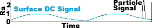
The limitation of particle detection on the wafer surface is affected by the level of background noise a photo detector picks up during the laser surface scan of a wafer. Similar issues affect scanning the surface of a quartz mask or film deposited wafer, which is discussed below. Background noise or surface roughness is a composite DC noise signal generated as the laser scans the silicon wafer surface, detected by the optical system. When that laser beam encounters a particle on the wafer surface, the laser scatters a larger AC signal pulse, detected by the photo detector.
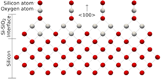
The DC signal from the photo detector (CCD) constantly changes due to is generated as the laser scans the surface of the polished wafer surface. The surface, although highly reflective to the human eye, is a mechanically polished surface and has surface roughness that can be measured and monitored during the production of the silicon wafer. Surface roughness is also increased by the organic oxide growth on the silica surface of the wafer, which adds to the DC electrical noise detected by the optical system. Unwanted Oxide growth on a silicon wafer is caused when oxygen reacts to the silicon substrate, forming a Silicon Dioxide (SiO2) film layer on the silicon surface, increasing surface roughness.
The 6 electrons of the oxygen atom literally pulls the silicon electrons to the oxygen atoms, forming a very strong SiO2 film layer on the wafer surface. Since a Calibration Wafer Standard is deposited with NIST Traceable particles on a prime silica surface, then over time, an SiO2 layer will grow as a film on that wafer surface, increasing surface roughness and increasing the DC noise signal output from the photo detector, making 10nm to 20nm particles even more difficult to detect, as the SiO2 layer grows in thickness. This phenomenon can shorten the life of a Calibration Wafer Standard to 3 years or less.
As a wafer inspection system scans the wafer surface, the photo detector produces a dc signal output, which increases/decreases in amplitude as surface roughness improves or worsens. The goal of scanning a substrate would be “0” microvolts of DC signal, frequently measured as Ra (roughness average). 0 microvolts (0 Ra) would be a near perfect surface.
Certainly, a desirable goal, but production technology does not allow for a perfectly polished silicon surface in 2025. Film deposits on the silicon surface, such as a Titanium Nitride or Titanium oxide, only increases this unwanted surface roughness effect during a laser scan of the wafer. As you decrease the particle diameters to be deposited on the wafer surface, the AC particle signal becomes much more difficult to isolate in the DC surface roughness noise, as detected by the photo detector.
Particle Detection
Detection of a particle is the discrimination between the AC pulse and the constant DC noise background. Large particles scatter a significant AC signal, and the photo detector can easily identify large particles. As the particle decreases in diameter, the laser scatter reduces in amplitude by the 6th power of the particle diameter, so S/N becomes quite difficult on newer SSIS tools operating from 18-30nm in particle size detection sensitivity.
Film deposited wafers also introduce a secondary scatter of the silicon surface that can be out of phase with a particle signal detected on the film surface, canceling out certain sized particles at certain film thicknesses and film types. Typically, the particle size detection on bare silicon surface is much better then on film deposited surfaces, due to S/N ratio; where an unpatterned silica wafer has a much better S/N than a film deposited wafer, due to increased surface roughness introduced by the film deposition on the silica surface.
Depending on the level of sophistication of the different SSIS tool, each wafer inspection system’s particle size sensitivity, i.e., the smallest particle it is specified to detect, all comes down to how well it can isolate a microvolt AC pulse in a sea of DC noise. The DC signal could be undulating like the waves in a calm sea, typical of a new ultraclean, polished wafer. But after an oxide film or titanium film is deposited on the wafer, the DC scatter can be much choppier at the microvolt level, making a 20nm particle signal extremely difficult to be detected by the photo detector.
SSIS Particle Size Calibration
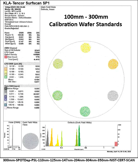
Above is a Calibration Wafer standard produced on a 300mm wafer with 6 size peaks beginning at 110nm particle diameter. No matter what tool, which company, which country; the calibration size peak at 110nm and the other 5 size peaks on this particular wafer standard (125nm, 147nm, 204nm, 304nm, 350nm) are all NIST Traceable. Every Wafer inspection System designed to a particular specification that is to be calibrated to these 6 size peaks, should respond with similar particle size response. Not a perfect response, but within 1 or 2 nanometers of each peak. So, a Calibration Wafer Standard can be specified with particle diameters of 1 to perhaps 10 different NIST Traceable size peaks in support of a particular tool design. And all tools of that design, calibrated to those NIST Traceable particle diameters, should respond with similar particle size data collected on similar production wafers. Therefore, the particle data collected during an IC production process, given a common size calibration reference, can be analyzed and discussed by Metrology Engineers at different manufacturing sites around the world, all with a goal of reducing particle contamination in their production process.
The curious anomaly, when scanning a wafer standard on two different SSIS tools is that particle counts can vary from machine to machine even though size diameter calibration is very precise. Counting differences is the result of laser beam power variations between any two machines: beam uniformity, age of laser, beam angle, etc. For example, older SSIS tools have a normal angle of incidence, designed with a red laser at 632.8nm wavelength; while more advanced SSIS tools today have a low angle of incidence with a blue laser at 480nm wavelength or a UV Laser at much lower wavelengths. Beam power, wavelength, beam angle, beam power uniformity and beam widths differ significantly between tools. When calibrated, the two SSIS tools should report identical size response, but may report different particle counts at each size peak. So many modern SSIS tools have added a count factor in their software that allows for the automatic adjustment of the count response, so that two different tools provide similar counts for calibration purposes.
SSIS tools from different manufacturers have a specified beam scan angle, beam power, beam uniformity, beam wavelength to meet the design objectives and customer’s scanning needs. Each tool ages over time, so proper maintenance and timely maintenance is required for long life and repeatable particle data.
In 2000 timeframe, a contamination particle was 250nm in diameter, whereas in 2025, semiconductor line geometry is approaching 3nm line width in R&D, and 18-20nm in production. 300mm wafers used in today’s production process must have very low particle counts of perhaps 20 particles on the entire 300mm wafer surface at 18nm particle diameter and above. Just for comparison, a human hair is on average 50 to 120μm in diameter – 50,000 to 120,000nm. Producing IC chips requires a particle free, ultra clean surface, with very few nano-particles on the substrate surface, which are 10,000 times smaller than the average human hair thickness.
The SSIS tool receives a constant flow of DC and AC data, as the wafer (mask or film-deposited wafer) is scanned over the wafer surface by the specified laser, the system’s optical system (photo detector or CCD) receives the AC/DC signal data at each moment of time. The SSIS tool’s software sorts out the data received for particle size, assigns X/Y coordinate particle location to each particle, sums the particle information to produce a bar chart with counts at each size range, stores the information to file for historical reference and statistical analysis over time, then displays the data as a color, topographical map of the wafer scan. Modern SSIS tools have incorporated wonderful features such as statistical analysis, HOST interfacing to a mainframe computer, faster response, etc.
Semiconductor chips produced today require clean environments that are far, far cleaner than any hospital operating room, now or in the future. The entire front-end production process of an IC chip produced on a 300mm wafer requires HOST Computers to manage the wafer movement with robotic control, while processing the silicon wafer with up to a 1000 different process steps with hundreds of different front end process tools, with each process step building a 3D IC chip geometry on a nanometer scale. Skin particles and hair on a 150mm, 200mm or 300mm wafer surface would shut down an entire IC production line!
Wafer inspection of the silicon wafer may be incorporated into a process step in a particular IC production process, but wafer inspection is certainly used to monitor the cleanliness of production wafers and the machines coming in contact with those wafers in an IC manufacturing process. In addition, the pre-inspection of the wafer is critical to sort out the clean silicon wafers that can be used in production from the bare silicon wafers that are not sufficiently clean to start the IC process. How then is the wafer inspection tool able to accurately detect and measure the particle diameter of these nanometer sized particles?
Surface Particle Sizing Variations in Wafer Inspection Systems
In 1990, wafer inspection design was focused around a normal angle of incidence, (a 90 degree beam angle) with a red, 632.8nm laser wavelength, detecting particle sizes of 500nm and above. As particle size sensitivity became more demanding down to 100nm, the angle of incidence changed to a low angle and laser wavelength moved to a blue laser at 480nm wavelength. More laser power at a low angle of incidence moved particle detection sensitivity down to 80nm in particle diameter. In 2015 timeframe, technology pushed the laser wavelength to UV wavelengths of 355nm and Deep Ultraviolet wavelengths down to 193nm with more narrow beam spots. This correlates to more power density in a smaller beam width to detect ever smaller particle diameters in IC production using 18nm to 80nm line geometry. Particle Detection Sensitivity of UV and DUV based SSIS tools gets particle size sensitivity down to the 30nm particle size range.
Brief Discussion on Wafer Inspection Systems (Surface Scanning Inspection Systems)
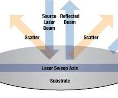
Basically, a Wafer Inspection System or Surface Scanning Inspection System (SSIS), scans the surface of a prime silicon wafer to detect and quantify unwanted particles using a red, blue or UV laser based scanning system. The beam width and beam power of the laser is constant, and the wafer typically spins under the laser, while the laser is moved outward from the wafer center to the wafer’s edge. As the laser strikes the wafer surface, the roughness of the silicon polish at an Angstrom level generates a dc signal noise. The laser scatter is detected by a photo detector. As the laser beam reflects off the silicon surface (or perhaps a quartz mask or film deposited surface), the reflected laser beam is scattered according to the level of surface roughness encountered at any moment, and the photo detector converts this laser scatter to a dc signal output. When a particle is encountered, the laser scatter produces an AC signal pulse as an output from the photo detector; which directly relates to a correct particle diameter, based on the size calibration of the SSIS tool.
It is this DC surface roughness signal that inhibits an SSIS tool to detect ever smaller particles. A 300mm wafer has a typical polish level measured to 5 angstroms (Å) Ra, which is ½ nanometer in surface polish, yet a 300nm wafer is hard pressed to be cleaned better than 18nm in particle diameter, forcing the IC production process to use line geometries of 18nm to 80nm for IC processing on a 300mm wafer. A 200mm wafer is polished to a typical 10 angstroms (Å) Ra, a 1nm surface polish, while a 150mm wafer polish is perhaps 20 angstroms (Å) Ra, a 2nm undulation. The surface roughness of the silica polish then has quite a negative effect to the detection of ever smaller micro-particles on the wafer surface.
Deposition of Microspheres on the Substrates
The first step in Particle Deposition is using clean, prime silicon wafers, quartz masks or customer supplied film deposited wafers. Particle sizes to be deposited on the wafer standard is dependent on the substrate diameter and level of cleanliness on the wafer surface. It would illogical to deposit 100nm particles on a 150mm wafer, since the surface polish and the surface cleanliness of a 150mm wafer is not nearly smooth enough in polish, nor clean enough to see 100nm particles on the surface. A 100mm wafer could have a maximum of 4 sizes deposited on the 100mm wafer surface, with 500nm the smallest particle deposited.
A 500mm wafer could have a maximum of 4 sizes deposited on the 150mm wafer surface, with 250nm the smallest particle deposited. A 200mm wafer could have a maximum of 6 sizes deposited on the 200mm wafer surface, with 80nm the smallest particle deposited; and 300mm wafers could have 10 sizes deposited on the wafer surface with 18nm being the smallest particle deposited. Each of the particle size limitations is based on the level of polish and level of surface cleanliness of that wafer diameter production.
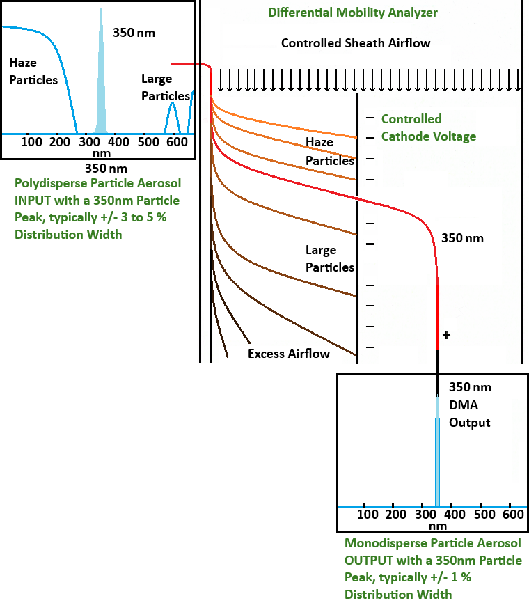
The image above describes a basic design of a particle deposition system in which a Differential Mobility Analyzer (DMA) is the key scientific tool used to isolate a narrow particle size peak on the output of the DMA, using very fine control of an electrode voltage and airflow velocity. The input to the DMA is a composite particle spectrum generated by an upstream atomizer (not shown).
The atomizer output includes the desired size peak as an aerosol, but in the creation of the aerosol, the aerosol stream generates unwanted nano-particles that are smaller than the desired size peak, double and triple charged particles and unwanted large particles above the desired size peak. The charged particles are neutralized upstream (not shown), but the DMA input still includes a variety of unwanted particles that can’t be deposited on the wafer. Using precise DMA voltage and airflow, the input aerosol enters the DMA. The voltage and airflow velocity are preset for a specified particle size
peak output. For this discussion, nano particles below 100nm enter the DMA, and the lower mass of the <100nm particles will be attracted to the cathode prior to the DMA output. The mass of large particles >100nm will travel past the DMA output and be collected by the cathode or be dumped into the exit airflow, depending on mass of the particle. Because a 100nm polystyrene particle has a very defined mass, the correct cathode voltage and airflow velocity allow the 100nm particles to escape thru the DMA output. But the DMA also has a refining affect to the particle size peak. The DMA is able to discriminate a very narrow portion of the size peak; thus, the size peak distribution width is narrower at the output of the DMA, than at the input of the DMA; and the unwanted large and small particles, above and below the size peak, have been stripped away from desired size peak. When depositing the 100nm particles (or any size peak from 18nm to 2µm onto a 300mm prime silica wafer, the size peak becomes a very precise calibration size point for SSIS tools.
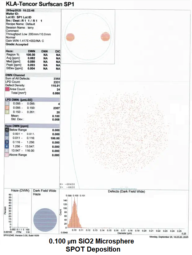
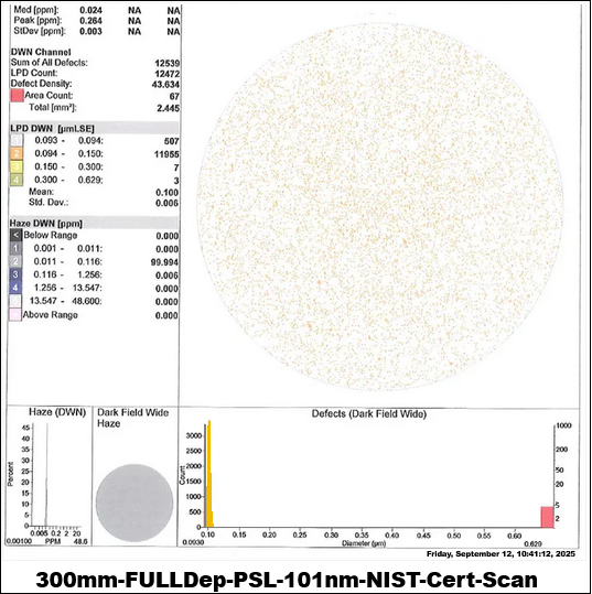
The particle Deposition specification may be 6 Spot Depositions (SPOT DEP), which is 1 particle peak deposited as a circle on the wafer surface at a defined location on the circumference of the wafer), in this discussion, on a 300mm prime silica wafer. The Wafer Standard Specification could be 10 SPOT DEPS from 30nm to 2µm on the 300mm wafer surface. In many cases the customer specification is for a single size diameter to be deposited on the wafer surface, a Full Deposition (FULL DEP).
A Full Deposition across the entire 300mm wafer surface is a uniform concentration of one particle diameter, and a FULL Dep wafer is a single calibration point for the SSIS tool, but the SSIS scan performance of the entire wafer surface by the SSIS tool can be analyzed. The detected particle diameter should not vary across the wafer, the size peak should be narrow, and by visually analyzing the wafer surface, one can determine if the SSIS tool has a constant particle detection of the uniform concentration of particles on the wafer surface.
A Spot Deposition on the wafer standard, across the entire wafer surface, is series of particle size peaks, typically starting at the notch, and each size peak deposited on the circumference of the radius at an equal distance from each spot. Six spot deps would be centered around the radius separated by 60 degrees, 10 spots at 36 degrees, 4 spots at 90 degrees, etc. The purpose of a SPOT DEP is to challenge the size accuracy
of the SSIS tool in one scan, across the full dynamic range of the SSIS tool. For example, a 200mm wafer may have 6 sizes deposited from 80nm to 2µm, so that the SP1 SSIS tool should correctly size all 6 size peaks in a single scan, otherwise the SP1 would require a calibration. An SPX tool might have 10 size peaks on a 300mm calibration wafer standard, and the SPX should correctly size each size peak, which are NIST Traceable and highly accurate in size diameter.
The DMA of the Particle Deposition System would normally be calibrated at the 4 SRM size references used around the world: 60nm, 100nm, 269nm and 895nm (see Section B above for polystyrene particle calibration). But Silica particles are also used for calibration, as silica is very resistant to shrinkage under the high laser power of modern SSIS tools. Polystyrene (PSL) and silica particles have a slight difference in refractive index. Silica particle size standards are available from 30nm to 2 microns. A 60nm silica microsphere will scatter differently than a 60nm polystyrene microsphere due to refractive index and translucence properties, although slight, so the calibration response curves are slightly different between a DMA Silica calibration and a DMA Polystyrene calibration. In either case, the DMA is calibrated with
polystyrene microspheres at 60nm, 100nm, 269nm and 895nm. A separate calibration curve for silica response of the identical 4 PSL sizes is saved into the PDS files to be used when depositing silica, as opposed to polystyrene.
By calibrating the Particle Deposition System using NIST SRM size references at the SRM sizes of 60nm, 100nm, 269nm and 895nm, the particle size response of the PDS system is very accurate in particle size for the production of Calibration Wafer Standards used by a wide variety of customers; all who have different Calibration Wafer Standard specifications.
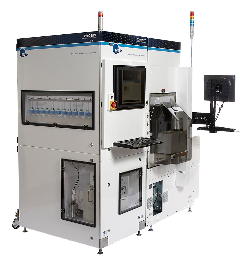
The 2300 NPT-2 Particle Deposition System at right used in our Particle Deposition Lab in the production of Calibration Wafer Standards, uses Recipe Control which includes all the operating parameters for the PDS to reproduce Calibration Wafer Standards to a specific customer specification for size accuracy, whether it is a single full particle deposition on a 100mm wafer or a Spot Deposition of 4-11 particle diameters on a 300mm wafer.
Recipe Control allows for many different “recipes” for a wide variety of Calibration Wafer Standards to be saved for future needs of any particular customer. The PDS tool is calibrated for NIST size diameter accuracy, thus reproduces very repeatable size accuracy on the calibration wafer standard, which is used to maintain size accuracy calibration on a wide variety of SSIS tools used in wafer IC Manufacturing fabs around the world.

