Calibration PSL Wafer Standards
Customer Review 0
★★★★★ 5/5
Our Calibration PSL Wafer Standards are deposited with polystyrene micro-spheres or silica microspheres, which support Metrology Managers that need to calibrate the size response of their Wafer Inspection Systems and Scanning Surface Inspection Systems (SSIS) with NIST Traceable size accuracy, using particle size standards with narrow size distributions.
Share it :
International Shipment
Your orders are shipped seamlessly between countries
30 Days Warranty
You have the right to return your orders within 30 days.
Secure Payment
Your payments are secure with our private security network.
Description
Calibration PSL Wafer Standards are a fundamental requirement for semiconductor metrology managers and calibration technicians who need to achieve precise, repeatable measurements from Scanning Surface Inspection Systems (SSIS). Your KLA-Tencor Surfscan, Hitachi, or Topcon SSIS tool is only as accurate as its last calibration. Our standards provide the absolute reference point you need to verify size accuracy, test count efficiency, and ensure the uniformity of every scan. Deposited with monodisperse polystyrene latex (PSL) spheres, these standards are the bedrock of a reliable semiconductor metrology program.
Key Specifications & NIST Traceability
Every standard we produce is a testament to precision. We provide a Certificate of Calibration traceable to NIST Standard Reference Materials (SRMs), ensuring that the measurements you take are anchored to internationally recognized standards.
- Particle Material: Monodisperse Polystyrene Latex (PSL) Spheres
- Particle Size Range: 20nm to 15 microns
- Peak Size Distribution: typically ≤ 3% for smaller sizes below 1um, greater than 3% for larger sizes
- Available Wafer Sizes: 75mm, 100mm, 125mm, 150mm, 200mm, 300mm
- Substrate Compatibility: Prime Silicon, Customer Quartz Mask, Customer Film Deposited Wafer
Deposition Methods: Full vs. Spot Deposition
The choice of deposition method directly impacts your calibration application. We offer both full and spot deposition to meet specific operational needs.
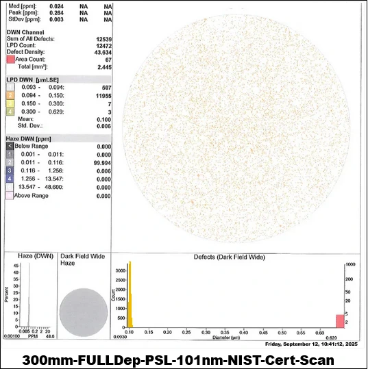
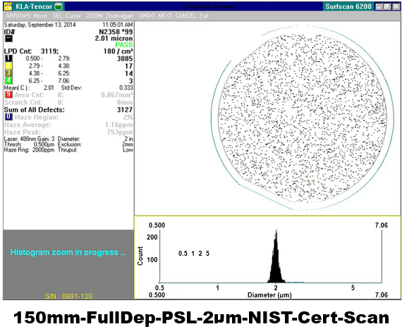
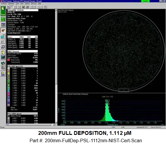
Full Deposition
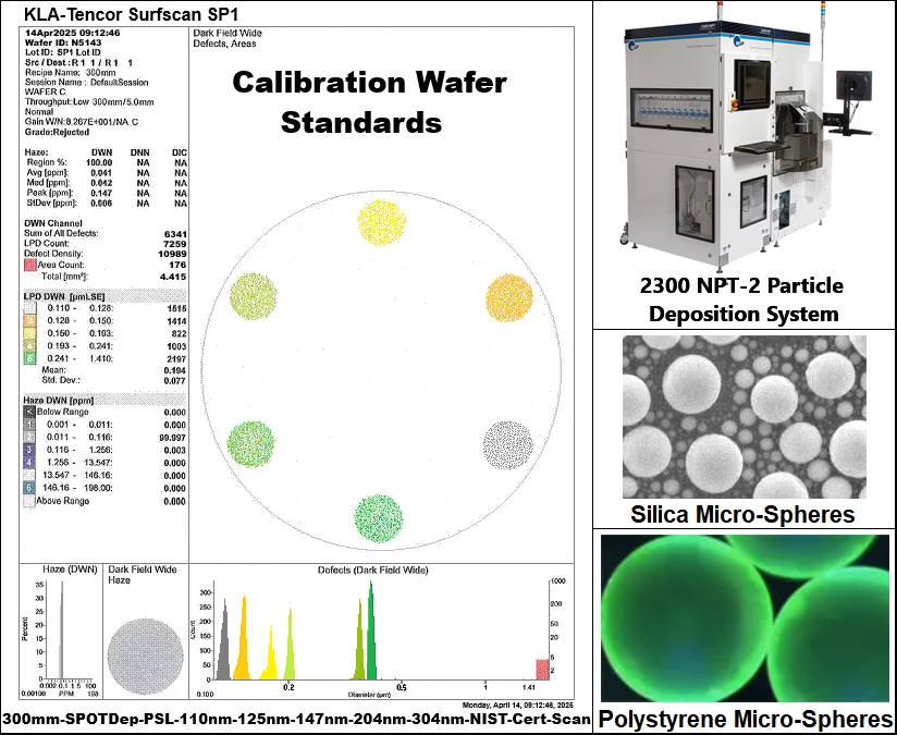
A full deposition standard involves laying down a single particle size across the entire wafer surface, leaving no portion undeposited. This method is ideal for verifying the scan uniformity of your SSIS tool. By challenging the system to detect particles consistently from edge to edge, you can identify and correct for variations in laser intensity or detector sensitivity across the wafer. It’s the most comprehensive way to evaluate the tool’s overall scanning performance. We’ve seen metrology managers use this to diagnose subtle, previously undetected issues in their Surfscan SP5xp tools, ultimately improving their process control.
Spot and Circle Deposition
Spot deposition concentrates PSL spheres in a specific, controlled location on the wafer, creating a visible spot. This technique offers two distinct advantages. First, it allows for the deposition of multiple, distinct particle sizes on a single wafer, making it a highly efficient standard for generating a full size response curve. Second, for contamination monitoring, the defined location provides an immediate reference point, improving count accuracy by eliminating ambiguity about where the tool should be looking. A technician once told me they cut their calibration time in half by switching to a multi-spot wafer for routine checks on their ADE inspection systems.
Advanced Deposition Technology
The quality of a PSL wafer standard is defined by the technology used to deposit the particles. We utilize two primary methods, each with its own strengths.
Direct Deposition
Our direct deposition method involves atomizing a solution containing monodisperse PSL spheres, mixing it with a highly filtered airflow (typically dry nitrogen), and depositing the aerosolized particles directly onto the wafer substrate. This process is highly effective and less expensive, making it an excellent choice for particles in the 1 µm to 12 µm range. It’s particularly well-suited for creating standards used to calibrate tools that monitor for larger contaminants.
Differential Mobility Analyzer (DMA) Controlled Deposition
For the highest level of precision, especially in the sub-micron range (50nm to 1 micron), we employ our Model 2300XP1 Particle Deposition System or 2300NPT Deposition Systems. These systems use DMA (Differential Mobility Analyzer) technology, which functions as a highly sensitive, particle size filter.
The process starts with an aerosol of polydisperse PSL spheres. This aerosol is charge-neutralized, and then passed through the DMA. By applying a precise voltage, the DMA isolates particles of a very specific electrical mobility, which corresponds to a narrow size peak. This technique physically strips away background particles and removes unwanted doublets and triplets (clumped particles) that can skew calibration results. A Condensation Particle Counter (CPC) monitors the count in real-time, allowing for automated recipe control and unmatched particle size deposition accuracy. This is the technology required to create a true 102nm standard with a distribution width under 3%.
Applications and Equipment Compatibility
Our Calibration PSL Wafer Standards are engineered to support the critical functions of semiconductor metrology and are compatible with a wide array of industry-standard inspection tools.
Primary Calibration Functions:
- Size Response Curve Calibration: Establish an accurate size response curve for your SSIS tool.
- Size Accuracy Verification: Routinely verify the measurement accuracy of your inspection system.
- Uniformity of Scan Evaluation: Test the scanning uniformity across the entire wafer surface.
- Count Efficiency Testing: Determine and track the particle count efficiency of your tools.
Compatible Inspection Systems:
- KLA-Tencor: Surfscan SP1, SP2, SP3, SP5, SP5xp, and the 6200, 6220, 6420, 6440 series.
- Hitachi: Full line of SSIS tools.
- ADE & Topcon: Wafer inspection systems.
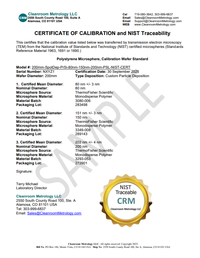
CRM-CERT-Sample
Frequently Asked Questions (FAQ)
What is the standard calibration method?
The standard method involves using a reference material with a known value (our PSL wafer standard) to challenge an instrument. The instrument’s response is then adjusted to match the known value of the standard, ensuring its measurements are accurate.
What are the three types of calibration?
While there are many specific procedures, they generally fall into three types: 1) Comparison Calibration, where an instrument is compared against a more accurate reference standard (this is how PSL standards are used), 2) Discipline Calibration, performed by a specialist in a specific field like dimensional or electrical metrology, and 3) In-situ Calibration, performed on-site without removing the instrument from its operational environment.
What is the 10 to 1 rule of calibration?
This is a metrology guideline suggesting the calibration standard you use should be at least ten times more accurate than the instrument you are calibrating. This ensures that the uncertainty of the standard itself is an insignificant factor in the final measurement. A 4-to-1 ratio is also widely accepted.
What are the 5 requirements for a calibration standard?
A true calibration standard must be: 1) Traceable to a national or international standard (like NIST), 2) Have a known and documented uncertainty, 3) Be stable over time, 4) Have properties relevant to the instrument being calibrated, and 5) Be acompanied by a formal certificate.
What is calibration as per ISO?
As defined by the ISO, calibration is the process of establishing a relationship between the measurements from an instrument and the known values of a reference standard. This operation is done under specified conditions and is used to identify and correct for any deviation in the instrument’s accuracy.
What is the standard for calibration in a lab?
The primary international standard for a calibration laboratory’s competence is ISO/IEC 17025. This standard outlines the technical and quality management requirements a lab must meet to prove it can produce valid and reliable resuts.
What is the difference between ISO 9001 and 17025 calibration?
ISO 9001 is a general quality management standard applicable to any organization. ISO 17025, however, is specific to the technical competence of testing and calibration labs. A lab can be ISO 9001 certified for its processes but must meet the much more rigourous technical requirements of ISO 17025 to be considered a competent calibration authority.
What is the difference between ISO and NIST calibration?
NIST is a U.S. national metrology institute that produces physical standards (SRMs). ISO develops international standards for processes and systems, such as the requirements for a calibration lab (ISO 17025). A calibration is “NIST traceable” if it can be linked back to a NIST SRM through an unbroken chain of comparisons.
What are the ASTM calibration standards?
ASTM International provides thousands of technical standards for specific industries and materials. While ISO/IEC 17025 governs the lab’s competence, an ASTM standard might dictate the exact procedure for calibrating a specific type of instrument, for example, ASTM E797 for calibrating spectrophotometers.
What is the NIST standard for calibration?
NIST (National Institute of Standards and Technology) provides Standard Reference Materials (SRMs) that serve as the physical basis for calibration in the U.S. For particle size, this means using certified materials, like our PSL spheres, whose physical properties have been characterized by NIST to ensure traceability.
What is ISO 17065 standard?
ISO/IEC 17065 is a standard for bodies that certify products, processes, or services. While ISO 17025 applies to the lab performing the calibration, ISO 17065 applies to an organization that would certify that a product, like a PSL Wafer Standard, conforms to its stated specifications.
Additional information
| Weight | 2 kg |
|---|