A. Integrated Circuits (IC Chips)
Semiconductor integrated circuits are built to meet a specific set of computer functions, such as process, RAM, buffer, etc. The integrated circuit is composed of intricate electrical conduction lines, connecting a variety of semiconductor process circuits (transistors) within that IC chip, which defines the circuit functionality of that IC chip. The semiconductor chip below shows a basic Integrated Circuit (IC) with the finished “front end” IC circuit in the middle, connected to the “backend” package via wires soldered between the IC chip and the IC package pins. The electronics of the IC chip sends and receives digital data through the wires into the pins, which are connected to the PC Board.
The older IC chips manufactured in the 1980s produced diodes, transistors and the Intel 8086 IC circuits on 100mm wafers using 2-3 µm wide conductive line traces with clock speeds of 6-8 mega-hertz (MHz). That was a dizzying clock speed then! Compare that 1980 speed to high-speed IC processing circuits produced today on 300mm wafers using 18 nanometer conductive line traces operating with 8+ giga-hertz (GHz) clock speed. 3 µm is 3000 nanometers, so in 40 years the integrated circuit geometry has shrunk by a factor of 3000/18 = 166.
More integrated circuits in the same space, operating at lower voltages, lower current demand, but much higher clock speeds in the giga-hertz range, approaching terra-hertz frequencies, far faster and smaller components than IC circuits produced 45 years ago.
B. Prime Silicon Wafer
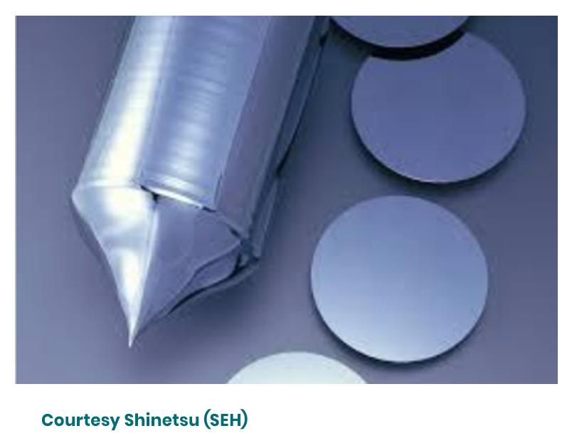
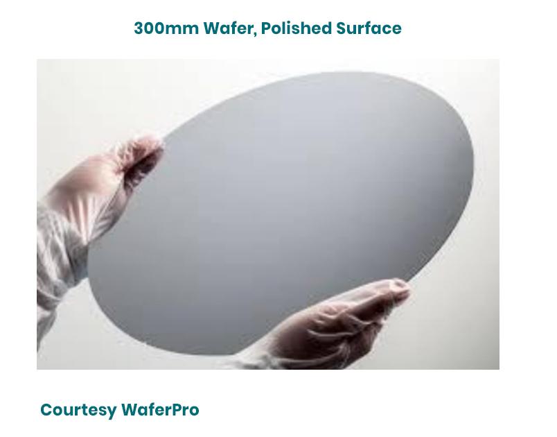
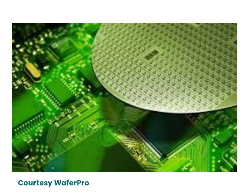
Integrated Circuits are primarily produced on silicon wafers. 100mm wafers were the predominant substrate used in the 1980s, followed by 125mm wafers, 150mm wafers, 200mm wafers (shown at right) in the 1990s, and then 300mm wafers beginning in the early 2000s. The silicon wafer manufacturing involves growing a large single-crystal silicon ingot using the Czochralski method, slicing it into discs, and then polishing and cleaning the wafers.
All silica wafer manufacturers have their intricate ingot growing methods; but we will not go into any detail crystal growing and slicing technology. The wafers are then processed by IC Manufacturers with process steps like doping, photolithography, etching, deposition, and ion implant deposition to design electrical conduction, impedance or isolation in the intricate patterns of IC microchips.
Companies such as Shinetsu (SEH) in Japan and Wacker Siltronic in Europe are well known around the world for their production of highly polished, ultraclean silicon wafers used in various semiconductor IC circuit manufacturing processes around the globe. In order to produce the integrated circuits on the silicon wafers, a very low particle count is required on the starting production wafers.
The surface of the wafer is what we are interested in, as the surface relates to particle detection and unwanted particle contamination, which directly affects the yield of integrated circuits produced on the wafer surface. Simply put, particles interrupt electrical flow in an IC circuit, thus a higher number of surface particles equals a lower yield of IC chips produced. Tens of thousand IC Chip designs are all affected by particle contamination, which limits the number of chips produced on a wafer. Product yield versus product cost!
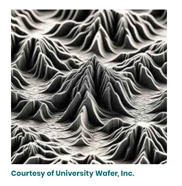
A polished 300mm wafer has a surface polish down to 2-3nm surface polish and undulations. We see a perfectly smooth surface, but the silicon surface at 3nm looks much different. The silicon wafer typically uses Chemical Mechanical Polishing (CMP) for semiconductor wafers, which uses a slurry to remove surface micro-damage to achieve an ultra-smooth, flat surface, which is what we see, a near perfect mirror. CMP is a semiconductor wafer process that uses a combination of chemical reactions and mechanical abrasion to flatten and smooth the rough silicon surface.
CMP is widely used in the semiconductor industry to create a near perfect planar (flat) surface by removing excess material and preparing the wafer for subsequent layers of circuitry to be added by hundreds of different complex process tools, each of which completes a single process step in the organic construction of the IC circuit.
A 200mm processed wafer may have as few as 89 very complex, large IC circuits designed on a single wafer; or as many as 35000 simple, small IC circuits designed on that wafer. Thousands of wafers producing that particular IC chip for a PC board designed to operate millions of computers, or to control the guidance of a ship, or used in the electronic system built into satellites that maintain GPS navigation. Every one of those production wafers are limited in performance by particles on the wafer surface. Detecting those particles requires sophisticated, laser based, wafer inspection tools.
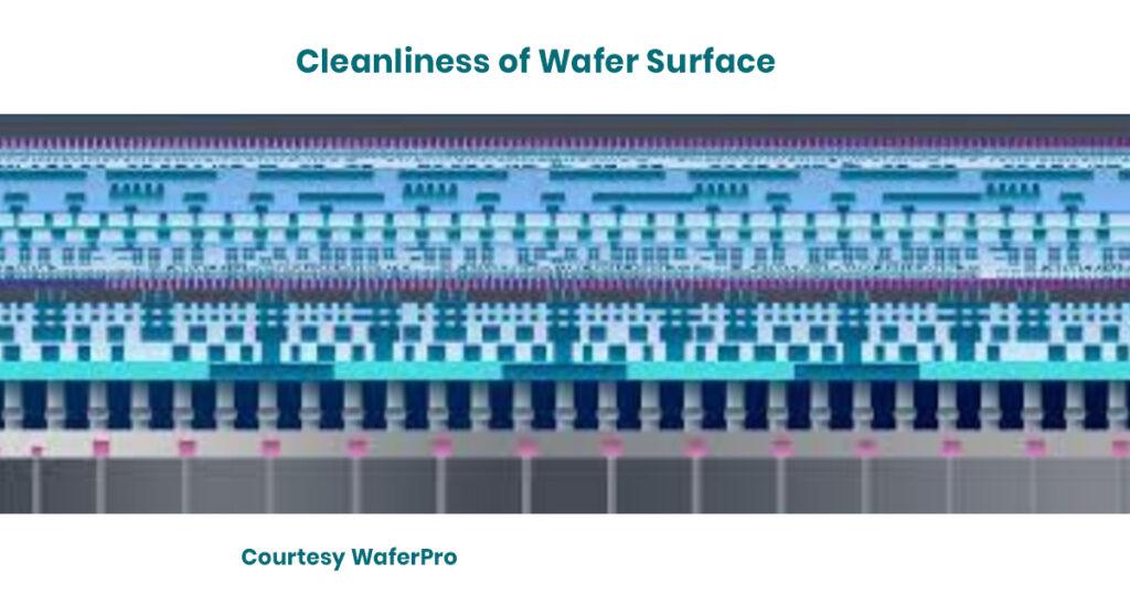
C. Cleanliness of Wafer Surface
Cleanliness of a prime silicon wafer prior to starting an IC process cycle is of very high importance. We think of a hospital operating room as clean; and they are! But an operating semiconductor cleanroom is far cleaner than the very best hospital operating room. Why? Each particle that lands on the wafer surface will interrupt the electrical conduction of a single process line that may only be 3-18nm in line width. Any one line of a single IC chip will cause that IC chip to be defective, thus a loss in product yield.
The Contamination Control objective of the Metrology Manager of any semiconductor fab is to reduce aerosol particles in the airflow, and to discover where particles come from that are detected on the production wafers. A 300mm wafer in today’s process lab will go through a 1000 process steps during a process evolution.
During each movement between process steps, the wafer travels in an enclosed FOUP carrier, never once contacting the open Class 1 or Class 10 airflow inside a fabrication facility. A FOUP is a ‘Front Opening Unified Pod’ used to hold 13 or 25, 300mm wafers during all process steps of an IC process; providing an ultraclean microenvironment of the 300mm wafers as the wafers move to each process machine via robotic handling.
In 1985, 100mm to 150mm wafers were moved from process machine to process machine by fully clothed (cleanroom smock, gloves, face mask, booties) technicians. In today’s 300mm IC process, the FOUP movement of the 300mm wafers and each process step of the individual 300mm wafer is controlled by a HOST computer. No human interface of the 300mm wafer occurs from start to finish. Each process step and each wafer movement outside of each process machine is controlled completely by the HOST computer. Where then do unwanted particles come from?
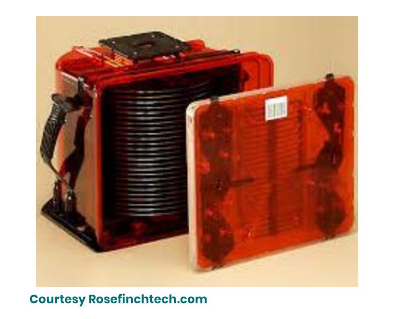
Particles migrate to a 300mm wafer surface in FOUPs, primarily from the internal surfaces of the FOUP itself, or residual purge gas, air turbulence/vortices during handling/docking. The 1st wafer (closest to the top, inner FOUP surface) is the most vulnerable wafer due to convection. Nanoparticles get agitated by airflow during purging of the FOUP or movement of the wafer from the FOUP to the process machine interface. Nanoparticles move within the sealed pod and settle onto wafer surfaces.
During the movement of the wafer from the FOUP into the process area inside the process machine, there is the possibility of particles landing on the wafer surface. Particles migrate to the wafers in process tools from various sources, such as tool wear (etching, grinding), contamination from handling (FOUPs, robots) and airborne nanoparticles. Once the wafer is inside the process tool, unwanted particle contamination may occur within a process step, for example during a wafer ion implant, lithography, photo resist, etching, oxidation, metallization process step. The particles may settle on the wafer surface due to gravity, electrostatic attraction, or being carried by gas/liquid flows via through thermophoresis or Brownian motion also playing roles, leading to surface contamination.
Process tool makers do everything they can to minimize mechanical occurring contamination onto the wafer, but they also have to pay attention to the process, which may generate aerosol particles that land on the wafer surface. The IC process itself may create surface particles during the process step. Unwanted particles generated during front-end integrated circuit (IC) processing are a major source of yield loss and can be broadly categorized by their origin and composition. In order for the Metrology Manager in the IC Fab to track unwanted particle contamination on wafer products, the Metrology Manager must collect the particle data based on each process step, so as to identify tools that may simply require a maintenance, or more importantly, discover a tool that is operating out of specification, in terms of mechanical contamination, or process introduced particle contamination.
D. Standards Introduced for IC Fab Operation
The FOUP was a physical product as manufactured by many companies (all to one interface specification) result of standards, which defined a method to store wafers in a common carrier during IC production in a robotically controlled IC Fab wafer process.
The SEMI E10 Standard for Reliability, Availability, and Maintainability (RAM) was created to measure machine uptime, availability for operation and downtime on process tools in the semiconductor industry, providing a universal language and methodology for defining, measuring, and tracking. The SEMI E10 Standard established six core equipment states (Productive, Standby, Scheduled Down, Unscheduled Down, Engineering, Non-Scheduled) and metrics like % Utilization and Mean Time Between Failures (MTBF), enabling consistent performance analysis between users of the process tools, as manufactured by the process tool equipment suppliers.
With regards to measuring particle contamination on the wafer, the important document to be familiar with is SEMI E14 – Measurement of Particle Contamination Contributed to the Product from the Process or Support Tool.
E. Particle Detection on Silicon Wafer Surface
Particles on a bare silicon wafer are detected using automated optical inspection systems (like laser scattering), referred to as a ‘Wafer Inspection System’ or Surface Scanning Inspection System (SSIS); where a laser scans the surface of a rotating wafer. As particles are illuminated, particles scatter the light, creating bright spots detected by photo Detector sensors (dark-field), scattered from the mirror-like surface, allowing for high-speed mapping and sizing of particles on the wafer surface.
Any two SSIS tools might scan the same wafer and provide two different sets of particle data, in terms of particle size and particle counts at each size. SSIS tools manufactured from 1980 to 2000 typically used a red laser at 632.8nm wavelength and at a 90-degree angle to the wafer surface (Normal Angle of Incidence). There were as many as ten different SSIS manufacturers around the world in the 80s and 90s, so SSIS particle size calibration became an important goal. A thousand IC Fab facilities around the world, with as many as 30 different SSIS tools in each Fab, forced the issue of particle size calibration of SSIS tools. SEMI Standards was formed as a result of the many demands of the IC Fab Managers to force Process Tool Manufacturers to provide standardization on many different aspects of the tools being produced.
After FY 2000, SSIS tools had to improve particle detection sensitivity since IC line widths were getting ever smaller in diameter. SSIS tools began using a low angle of incidence for laser illumination, while changing the red laser wavelength from 632.8nm to a blue laser at 488 nanometers wavelength to achieve more power on the wafer surface. In 2025, SSIS tools are now using UV Lasers at wavelengths of 355nm. Deep UV (DUV) lasers at 266 nm do not penetrate deeply into silicon-on-insulator (SOI) structures, as longer wavelengths do (like the older 488 nm Ar+ laser). This avoids noise from internal reflections and interface roughness within the wafer layers, improving the signal-to-noise ratio, as discussed below.
Particle Size Calibration of an SSIS tool is critical. As noted above, thousands of SSIS tools, produced by a variety of manufacturers around the world, all have to calibrate their tools to NIST Traceable, size standards. The SEMI E14 document is the standard by which tools are calibrated. All SSIS tools have their individual calibration routines, but the tools need to conform to a common size calibration response, so that IC Fab Metrology Managers have a common reference to derive particle data. A one-micron silica microsphere should size the same as a 1-micron polystyrene microsphere. For SSIS calibration purposes, microspheres are used, where perhaps 4 size points between 100 nanometers and 1 micron are used to create a size response curve in the SSIS tool. The SSIS tool might have upwards of 20 different calibration curves stored in memory for use with a variety of IC contamination control goals in the Fab.
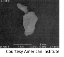
Calibration of the SSIS tool provides a nominal manner to collect particle data, yet the calibration of the SSIS tool is accomplished using microspheres, that are NIST Traceable. And the SSIS tools today are very good at sizing the standards and creating size response curves; yet unwanted process particles in an IC process, detected on an un-patterned monitor wafer or patterned process wafers, are not spherical, and have a variety of chemical origins. Common particles on 300mm wafers include silicon (Si) (SiO₂, SiC), metals (Cu, Fe, Ni), organic compounds, dust, fibers, and chemical residues, originating from equipment, operators, airflow, or processes, with tiny nanoparticles < 30nm being critical in today’s IC processes, but very difficult to detect, all having an impact to IC device yield.
Calibrating particle size on real process wafers is difficult due to particle shape/material variability, instrument limitations such as undersizing and oversizing, effects of doubly charged particles, and particle sampling differences of various SSIS tools. This requires particle deposition systems (PDS) capable of depositing polystyrene or silica microspheres from 18 nanometers to 15 microns. But the real challenge lies in bridging the gap between calibrating to idealized calibration microspheres and detecting complex, process particles on the wafer surface. Particle size accuracy is easily identified using calibrating microspheres, but much less accurate in size response when detecting real-world process particles on the wafer surface, which are rarely spherical. Particle shape and material variability are major challenges for particle sizing in wafer processing because most optical inspection tools are calibrated with microspheres of a known diameter and known refractive index. Real-world process particles are irregular in shape (fibers, agglomerates, fragments) and can be composed of diverse materials (metals, organics, silicon particles), leading to inaccurate size measurements and misinterpretation of defect types.
F. Surface Roughness Affects to Particle Detection Sensitivity
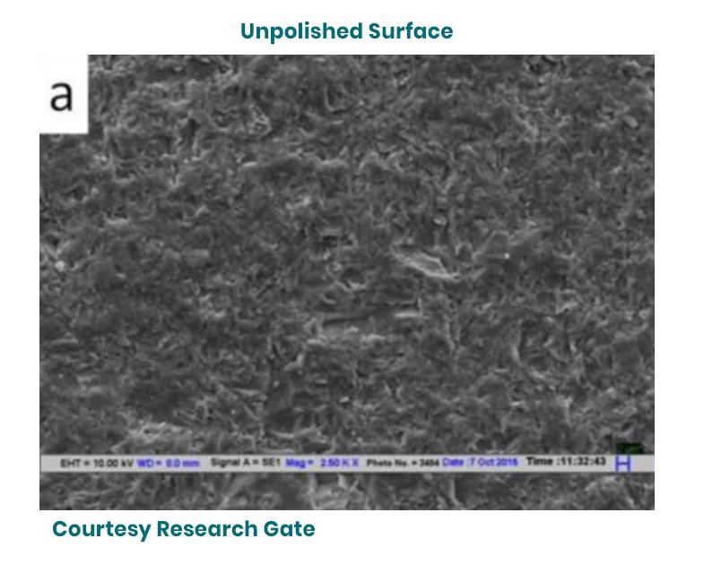
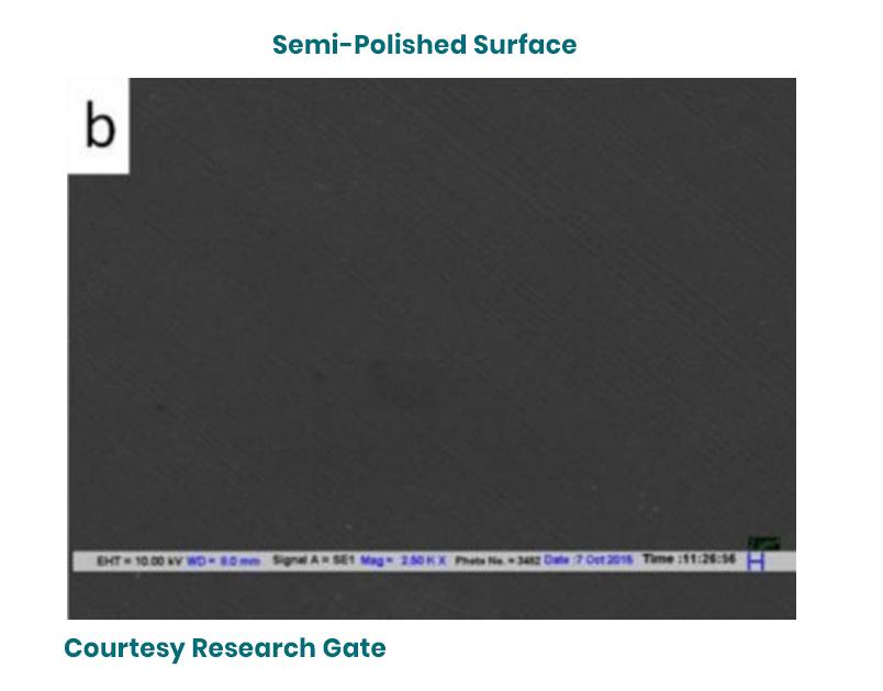
Surface roughness on a wafer significantly hinders particle detection, especially for nanoparticles, by scattering light and creating background noise (haze), making it hard to distinguish real particles from surface texture, especially as polish levels decrease and natural oxide layers grow, forcing more complex optical analysis or advanced techniques to separate signal from the inherent surface signal. Roughness creates topographical scatter that masks smaller particles, reducing sensitivity and throughput for defect inspection systems. The polished wafer surface looks like a perfect mirror, but when analyzed with TEM or SEM, the silicon surface is quite rough.
As a laser scans over the surface, the laser scatter produces a DC noise relative to the amount of surface roughness. A 300mm wafer is polished quite well, whereas the laser scatter (DC noise) on a 100mm wafer is far worse. Imagine a 10nm particle on a polished 300mm wafer. The particle could easily fall into the polish imperfections and never be detected above the DC noise boundary of the polish.
Rough surfaces scatter light in complex patterns (like “brown haze”), overwhelming photo detectors and obscuring small particles, making them look like noise rather than distinct defects. The scattered light from surface texture mimics the signal from actual particles, making it difficult for SSIS tools to discriminate the difference between a low amplitude AC signal pulse of a 10nm particle, detected in a sea of DC signal noise of the polished wafer surface. Poor polish increases surface roughness and lowers the particle detection sensitivity of SSIS tools. The SSIS system struggles to detect nano-defects because the background noise is too high, limiting surface particle detection to larger particles.
Once a wafer has been polished, a native oxide layer will begin to form, adding nanoscale roughness that affects detection sensitivity over time, complicating calibration of the SSIS tool, but this oxide layer grows slowly over time, yet as it grows in thickness, the smallest calibration particle, for example, a 20nm microsphere spot deposition, will be more difficult to detect over time. Surface roughness and oxide growth limits the life of a Calibration Wafer standard at the smallest size peak deposited on the wafer.
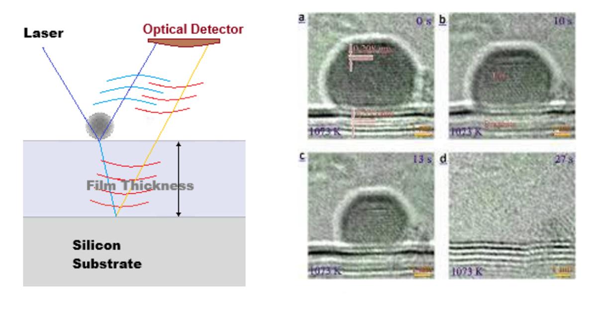
G. Film Thickness Affects to Surface Particle Detection
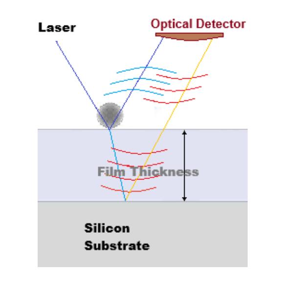
Film thickness significantly affects particle detection on a 300mm wafer by influencing the sensitivity of SSIS inspection tools, primarily through light scattering properties, signal-to-noise ratio, and the physical properties of the film itself. Most SSIS tools use laser scattering and the amount of light scattered by a particle depends on the film’s optical properties (refractive index, transparency) and its thickness. Films below a critical thickness might be “effectively invisible” from particle detection perspective, as the substrate’s properties dominate the signal.
But certain types of films and film thicknesses, for example SiO₂, may be completely invisible to the laser as it scans the wafer surface, yet, films such as TiO₂, Al₂O₃ or Si₃N₄, can lead to optical interference effects, which may either enhance or diminish the detection of a particle (on the film surface) against the film background. Certain types of films, at certain thicknesses can cause a doubling of the particle scatter from the particle on the film surface, or the opposite can occur where the particle scatter is nulled from two different signals of the same particle.
These nuances make particle detection on a film much more difficult at some thicknesses and easier at others. When a particle is encountered on a film, the primary laser scatter is a function of the particle. But a secondary signal will occur as the laser penetrates the film layer, strikes the silicon surface, then reflects upwards underneath the particle on the film surface. This may cause an “out-of-phase” scatter signal. The primary scatter signal would combine with the out of phase scatter, and cancel the particle scatter to the photo detector. Conversely, depending on the film type and thickness, the secondary scatter off the silicon surface may be in phase with the primary scatter signal, causing a doubling affect to the total scatter signal detected by the photo detector.
There are many different types of films deposited on the wafer, at various thicknesses. Depending on the film type, film thickness, laser wavelength, the “out of phase” scatter component causes the particle scatter to disappear from the optical detector, thus the particle is not detected. Yet it is clearly on the film surface. In other cases, the two particle signals are in phase and the particle on the film is detected by the photo detector larger than the actual particle size.
The IC manufacturer produces a variety of IC chips from complicated Microprocessors, Power Management chips, sensors, memory, etc. The industry has gone from 100mm wafer to 300mm wafers in order to produce more volume and lower cost per chip. It is a natural progression of device manufactures to reduce their costs, but as wafers were increased in diameter, the equipment suppliers had to redesign their process tools. A 100mm IC Fab could not be upgraded for 150mm wafers, so a new FAB had to be built and all new 150mm equipment had to be purchased, installed, tested, and then perhaps 1-2 years of implementing a new process to produce IC products on 150mm wafers.
In each evolution, the process tools became more computerized, more software, more complex in general, which increases the machine cost at each evolution on the supplier side. On the process side, the IC devices became far more complicated, smaller electrical line widths, more ICs on larger wafers. When 300mm wafers were introduced, the 150mm FABs could not support the much larger 300mm wafers on 150mm process tools, so another new FAB had to be built. IC Manufacturers around the world such as Intel Corp., Samsung Corp. AMD Corp, etc. had to go through these new FAB constructions and new process integrations to build new 300mm Fabs.
When 450mm wafers were introduced by the silicon wafer manufactures, the semiconductor industry was delirious. But then the equipment manufacturers and IC Fab Managers realized there is a point at which increasing the wafer sizes is controlled by the machine cost + Fab cost to put the larger 450mm wafer into IC production. As of 2025, that goal has not been achieved due to the staggering cost of building machines to handle the very large wafer surfaces, building totally new IC Fabs to install the new 450mm machines; and start creating new IC processes. Needless to say, 300mm IC production is where the industry has been for 10+ years, and perhaps for another 10 years.
Frequently Asked Questions (FAQs)
Why is a semiconductor cleanroom described as “cleaner than a hospital operating room”?
In a hospital, the goal is to eliminate biological pathogens. In a semiconductor cleanroom, the goal is to eliminate microscopic inorganic particles. Because modern IC line widths are as small as 3-18nm, even a single nanoparticle can bridge a gap and cause a short circuit, destroying the entire chip.
What is a FOUP and why is it used?
A FOUP (Front Opening Unified Pod) is a specialized plastic enclosure used to move wafers between process machines. It maintains an ultra-clean microenvironment, protecting wafers from the surrounding fab air and preventing human interface, which is a major source of contamination.
How has the geometry of integrated circuits changed over the last 40 years?
Integrated circuit geometry has shrunk by a factor of approximately 166. In the 1980s, line traces were 2-3 µm (3000nm) wide. Today, they are as small as 18 nanometers, allowing for significantly higher speeds (GHz vs MHz) and lower power consumption.
What is the difference between DC and AC signals in particle detection?
In laser scanning (SSIS), “DC noise” refers to the constant background light scattered by the surface roughness (haze) of the wafer. The “AC signal” is the sudden pulse of light scattered when the laser hits an actual particle. High DC noise can “hide” the AC signal of a small particle.
Why hasn’t the industry fully transitioned to 450mm wafers?
While larger wafers offer more chips per wafer, the cost of building new Fabs and the massive machines required to handle 450mm surfaces is currently prohibitive. As of 2025/2026, 300mm remains the industry standard due to this economic balance.
How do thin films affect particle sizing accuracy?
Thin films can create optical interference. Depending on the film thickness and the laser wavelength, the reflected light from the substrate can either add to the particle’s signal (making it look larger) or cancel it out (making the particle invisible to the detector).
