
Description
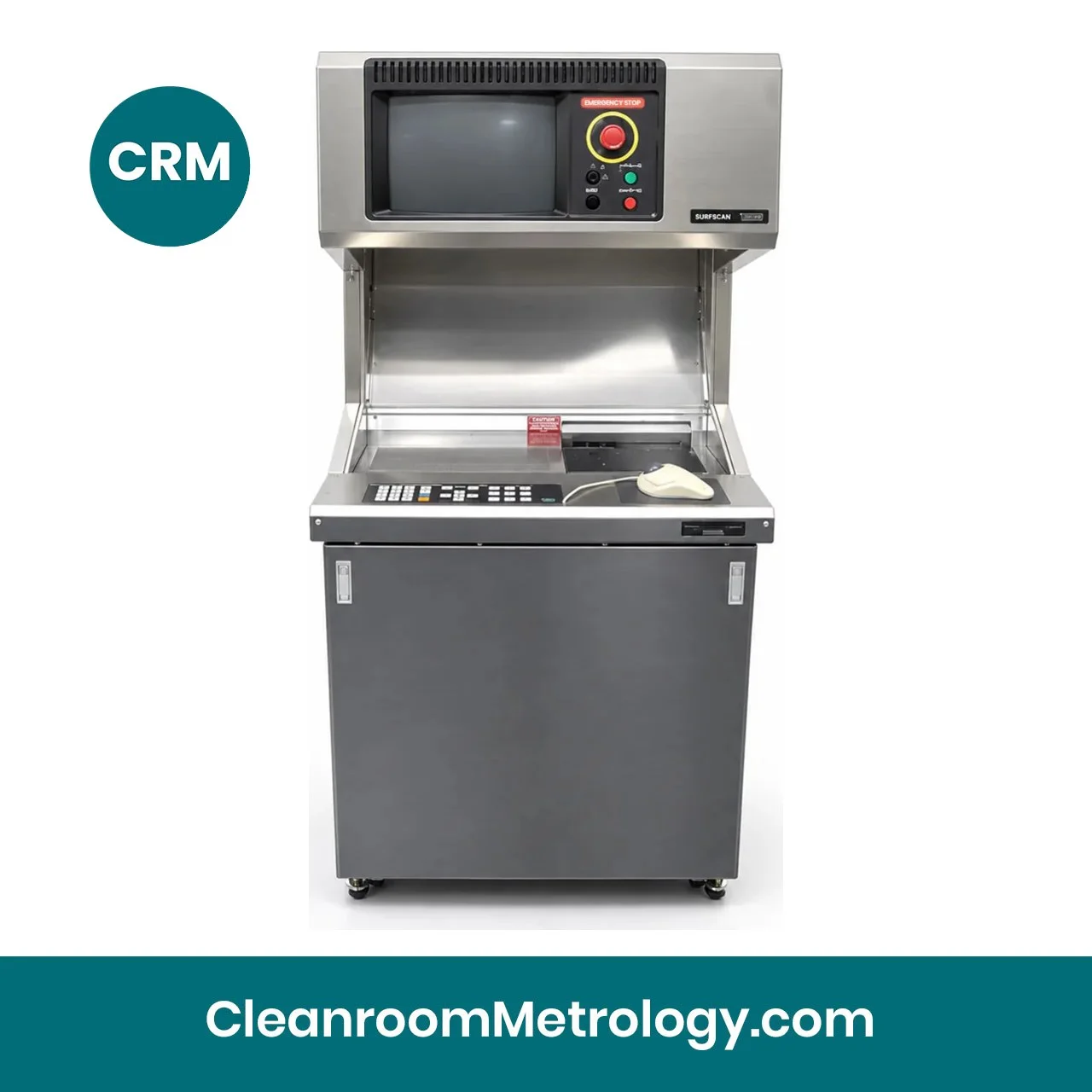
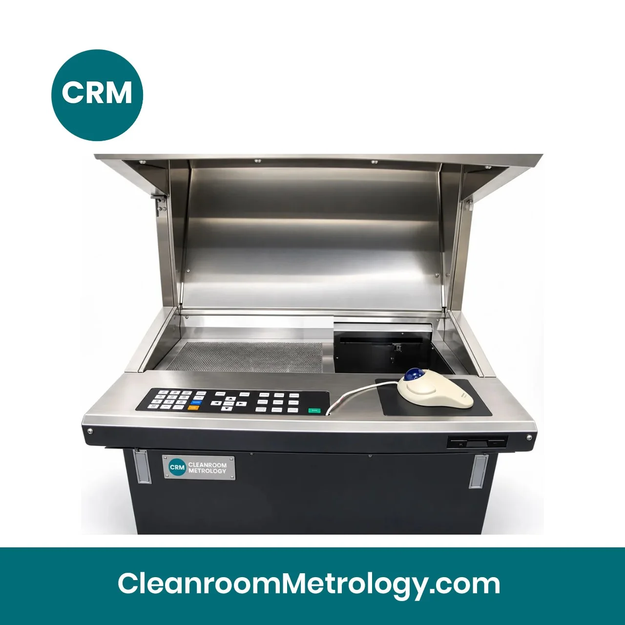
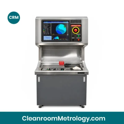
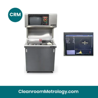
Tencor Surfscan 6100 for Particle Defect Inspection on Bare Silicon Wafers
| System Type | Tencor Surfscan 6100 Upgraded, unpatterned wafer surface inspection system (SSIS), refurbished |
| Particle Detection | ≈ 0.204 µm (204 nm) at a 95% capture rate on bare silicon |
| Laser | Red 632 nm laser; data matches Surfscan 4500 and 5500 tools |
| Wafer Size | Bare silicon wafers up to 200 mm (8 inch) |
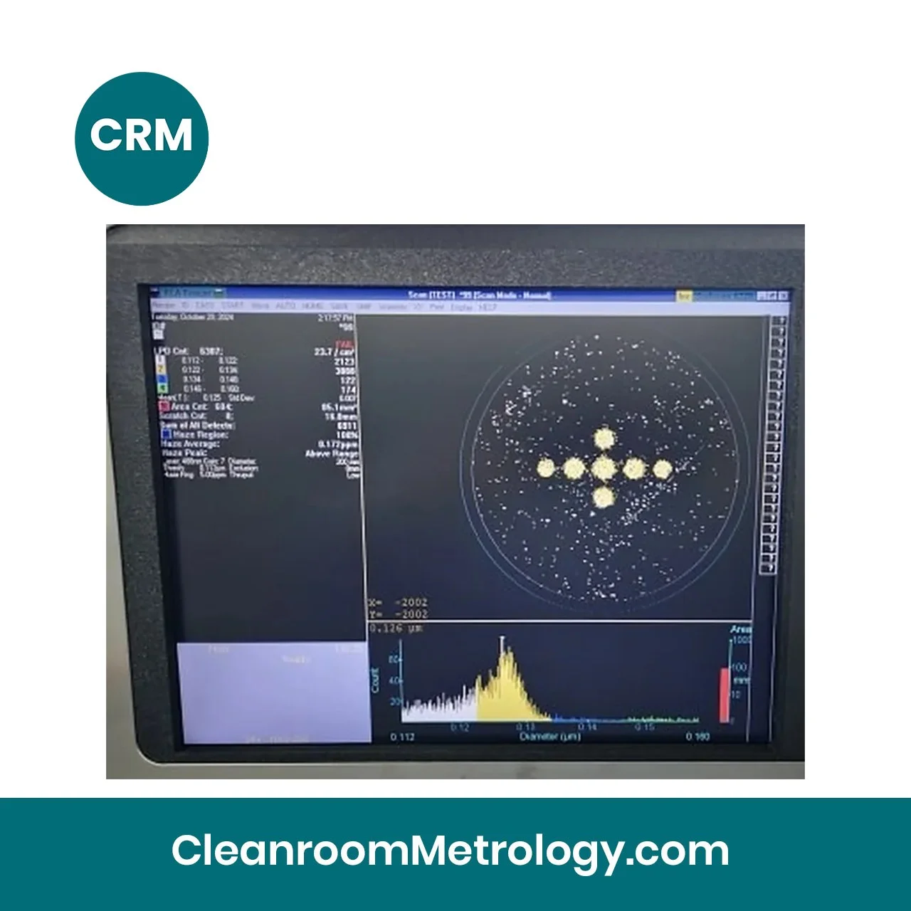
| Measurements | Particle (LPD) count, size and wafer map; haze-related (surface roughness) information |
| Data Output | Histogram, particle Data, Haze Data |
| Storage | Solid state hard drives |
| Calibration | NIST-traceable PSL calibration wafer standards |
| Warranty | 6 months Optional, parts, Onsite Installation Optional |
| Lead Time | January 2027 |
The Tencor Surfscan 6100 is a legacy optical inspection system for unpatterned wafers. A laser scans the bare silicon surface, and light scattered by each particle or surface anomaly is detected, counted and sized as a light point defect (LPD). The result is a particle count by size bin and a wafer map, which process engineers use for incoming wafer inspection, tool and process monitoring, and failure analysis. The 6100 is not designed for patterned-wafer inspection, small wafer pieces, quartz masks or glass slides.
This refurbished Surfscan 6100 Upgraded detects particles down to ≈ 0.204 µm (204 nm), and its red 632 nm HeNe laser produces particle size and Haze (surface roughness) data that correlates with older Surfscan 4500 and 5500 tools, so historical particle data stays comparable when you replace your Tencor 4500 or 5500.
Surfscan tools are also referred to as wafer particle counters, wafer surface scanners, defect scanners and SSIS tools. Cleanroom Metrology has supplied PSL Calibration Wafer Standards for SSIS calibration for 28 years, and every refurbished Surfscan we supply is calibrated against NIST-traceable PSL Wafer Calibration Wafer standards.
Why replace a Tencor Surfscan 4500 or 5500 with a refurbished Surfscan 6100?
Tencor Surfscan 4500 and 5500 tools are about 40 years old, and parts for them are getting difficult to locate. A failed PC board or laser can take an wafer inspection step offline for months. Moving to a refurbished Surfscan 6100 gives you a newer platform from the same Surfscan family, with upgraded PC Boards, system check and Particle Size Calibration; and can be set up for 75mm to 100mm wafers or 100mm to 200mm wafer. And the Tencor 6100 uses a red 632.8nm wavelength laser, same as with the Tencor 4500 and Tencor 5500, so your particle data stays comparable to the 4500 and 5500 particle results already in your records.
Data continuity matters because particle specifications, control limits and customer reports are usually built on years of historical scans. Changing to a tool with a different laser wavelength can shift reported particle counts and sizes, which forces a re-baseline of control charts. The red-laser 6100 avoids most of that work. The advantage: newer technology, available parts, much better particle sensitivity, comparable data output. Onsite installation and calibration is optionally available.
Compare the Tencor Surfscan 6100 Wafer Inspection System configurations
Need new boards, a new HeNe laser or SECS/GEM main boards? Compare the Tencor Surfscan 6100 Enhanced and the Tencor Surfscan 6100 Ultimate.
| Feature | Surfscan 6100 Upgraded | Surfscan 6100 Enhanced | Surfscan 6100 Ultimate | Surfscan 6220 Ultimate | Surfscan 6420 Ultimate |
| Particle detection on bare silicon | ≈ 0.204 µm (204 nm) at 95% capture rate | ≈ 0.16 µm (160 nm) at 95% capture rate | ≈ 0.16 µm (160 nm) at 95% capture rate | ≈ 0.12 µm (120 nm) at 95% capture rate | ≈ 0.100 µm (100 nm) at 95% capture rate |
| Haze (surface roughness) measurements / resolution | Yes, customer calibrates | Yes, customer calibrates | Haze down to 0.02 ppm, resolution @ 0.002 ppm | Haze down to 0.02 ppm, resolution @ 0.002 ppm | Haze down to 0.02 ppm, resolution @ 0.002 ppm |
| Laser and scan | Red 632 nm HeNe, gas tube laser | New, red 632 nm HeNe, gas tube laser | New, red 632 nm HeNe, gas tube laser | New, blue, solid state 488 nm laser | New, blue, solid state 488 nm laser |
| Optical detector | Photo-multiplier tube (PMT) | Photo-multiplier tube (PMT) | Photo-multiplier tube (PMT) | Photo-multiplier tube (PMT) | Photo-multiplier tube (PMT) |
| Incidence angle | Normal-incidence illumination for unpatterned silicon wafer defect detection down to 204 nm & haze (surface roughness) measurements | Normal-incidence illumination for unpatterned silicon wafer defect detection down to 160 nm & haze (surface roughness) measurements | Normal-incidence illumination for unpatterned silicon wafer defect detection down to 160 nm & haze (surface roughness) measurements | Normal-incidence illumination for unpatterned silicon wafer defect detection down to 120 nm & haze (surface roughness) measurements | Low-angle (oblique) incidence illumination for unpatterned silicon wafer defect detection down to 100 nm & haze (surface roughness) measurements |
| Main PC boards | Checked for system operation, engineering updates | Brand-new main PC boards supporting original design | Brand-new, improved main PC boards, optional SECS/GEM data output | Brand-new, improved main PC boards, including SECS/GEM data output | Brand-new, improved main PC boards, including SECS/GEM data output |
| SECS/GEM data output | Optional | Optional | Optional | Yes, SECS/GEM data protocol installed | Yes, SECS/GEM data protocol installed |
| Hard drives | Solid state | Solid state | Solid state | Solid state | Solid state |
| Optical mirrors cleaned and adjusted | Yes, optical system cleaned and adjusted for red 632.8 nm laser | Yes, optical system cleaned and adjusted for red 632.8 nm laser | Yes, optical system cleaned and adjusted for red 632.8 nm laser | Yes, optical system cleaned and adjusted for blue 488 nm laser | Yes, optical system cleaned and adjusted for blue 488 nm laser |
| Calibration wafer standards | Optional, 3 full-deposition calibration wafer standards, 220 nm, 500 nm, 1019 nm | Optional, 3 full-deposition calibration wafer standards, 204 nm, 500 nm, 1019 nm | Included, 3 full-deposition calibration wafer standards, 204 nm, 500 nm, 1019 nm | Included, 4 full-deposition calibration wafer standards, 126 nm, 304 nm, 700 nm, 1019 nm | Included, 4 full-deposition calibration wafer standards, 100 nm, 304 nm, 700 nm, 1019 nm |
| Installation and calibration | Optional onsite install, system check and size calibration | Optional onsite install, system check and size calibration | Optional onsite install, system check and size calibration | Optional onsite install, system check and size calibration | Optional onsite install, system check and size calibration |
| Windows print server | Optional | Yes | Yes | Yes | Yes |
| Warranty | 6 months optional, travel not included | 6 months optional, travel not included | 6 months included; extended optional, travel not included | 1 year included; extended optional, travel not included | 1 year included; extended optional, travel not included |
| Availability | January 2027 | January 2027 | 1st Quarter 2027 | 1st Quarter 2027 | 2nd Quarter 2027 |
Keep your tool running after warranty with a Surfscan parts contract, or browse all Surfscan wafer inspection systems.
FAQs about the Tencor Surfscan 6100 Wafer Inspection System
What can the Tencor Surfscan 6100 detect?
Particles down to ≈ 0.204 µm (204 nm) on bare silicon wafers, reported as light point defects with count, size and wafer map, plus haze-related surface roughness information.
Can it replace a Surfscan 4500 or 5500?
Yes. The 6100 uses a red 632 nm laser that matches 4500 and 5500 particle data, so your historical results remain comparable.
What wafer sizes does it handle?
Bare silicon wafers up to 200 mm (8 inch). It is not intended for wafer pieces, quartz masks or glass slides.
Is the Surfscan 6100 new?
No. It is a refurbished wafer defect inspection system with faulty components replaced, size calibrated and can be covered by a optional 6-month parts warranty.
Reviews
There are no reviews yet.